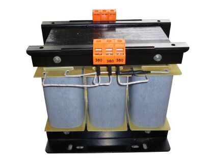
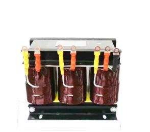
The power frequency AC power supply becomes a stable DC power after the transformer is stepped down, rectified, and filtered. The remaining part is the control part of voltage regulation and stabilization. After the power supply is connected to the load, the output voltage is obtained through the sampling circuit, and the output voltage is compared with the reference voltage.
If the output voltage is less than the reference voltage, the error value is amplified by the amplifier circuit and sent to the input of the regulator, and the output voltage is adjusted by the regulator until it is equal to the reference value; if the output voltage is greater than the reference voltage, it is passed through the regulator Reduce the output.

The three-phase automatic AC voltage regulator circuit is composed of =l2V power supply circuit, voltage detection and control circuit, and overvoltage protection. The l2V power supply circuit is composed of W4 and W5 windings of voltage regulating transformer T and rectifier diodes VDL-VD4, filter capacitors Cl, C2 composition. The voltage detection control circuit is composed of resistor R-R7, potentiometer RP, Rm, Zener diode VS, capacitor C3, C4 and operational amplifier integrated circuit IC (Nl-N3).
The overvoltage protection circuit is made up of N3, transistor V3, resistor Rl2, and relay K inside the IC. The automatic voltage adjustment circuit consists of resistors R8-All, transistors Vl, V2, DC motor M, sliding contacts, and T windings Wl-W3. After connecting the output terminal of the AC voltage stabilizer to the mains, an induced voltage is generated on the windings of W4 and W5 of T.
After this voltage is rectified by VDL-VD4 and filtered by Cl and C2, it provides an unstable working voltage of ±12V for IC and Vl, V2, etc. The +l2V voltage has other effects. After Rl-R3 voltage division and VS voltage stabilization, they respectively provide reference voltages for the inverting input terminals of Nl-N3; provide operating power for K and V3 of the overvoltage protection circuit; after R4, RP2, and R6 are divided, Provide the detection voltage for the non-inverting input terminals of Nl and N2; after being divided by R7, RP and R5, provide the detection voltage for the non-inverting input terminal of N3.
In the first part of the switching cycle, the input voltage is applied to a capacitor (C1). During the second part of the switching cycle, the charge is transferred from C1 to the second capacitor C2. The structure of the most traditional switched-capacitor converter is an inverter, in which C2 has a grounded positive terminal, and its negative terminal transmits a negative output voltage. After a few cycles, the voltage through C2 will be applied to the input voltage.

three-phase voltage regulator: automatic voltage regulator
Assuming there is no load on C2, no loss on the switch, and no continuous resistance in the capacitor, the output voltage will be exactly the negative of the input voltage. In reality, the efficiency of charge transfer (and the resulting accuracy of the output voltage) depends on the switching frequency, the resistance of the switch, the value of the capacitor, and the continuous resistance.
A similar topology voltage doubler uses the same switch and capacitor bank but changes the ground connection and input voltage. Other more complex variants use additional switches and capacitors to achieve other conversion ratios of input voltage to the output voltage, and in some cases, use specialized switching sequences to generate fractional relationships. In the simplest form, switched-capacitor converters do not have a voltage regulator function.
Some new semiconductor switched capacitor converters have an automatically adjusted gain level to produce a regulated output; other switched capacitor converters use a built-in low-dropout linear regulator to produce an unregulated output.